PCM_ISSCC_2012_4GB配置文件参数解析
本文的参考内容来自于MEMORY SYSTEMS Cache,DRAM,Disk这本书,作者为BRUCE JACOB,SPENCER W.NG,DAVID T.WANG。(链接)
首先了解几个概念,北桥称为系统总线,是内存传输的主要信道,因此速度比较快;南桥称为IO总线,主要联系硬盘、USB、网卡等设备。北桥支持的频率称为前端总线速度(每秒传输次数),而每次传送的bit数则是总线宽度,我们熟悉的总线带宽(总线速度x总线宽度)即为每秒可传送的最大数据量。
tBURST 4:数据burst的时间为4个周期
RATE 2:数据传输速率,每个周期两次传输
BusWidth 64:每次传输bit数,总线宽度(以bit为单位)
1 | wordSize = p->BusWidth; |
使用数据burst来提高数据吞吐量,burst长度=tBURST*RATE=8。
tRCD 48: Row to Column command Delay. The time interval between row access and data ready at sense amplifiers. 在进行数据的读写前,Controller 需要先发送 Row Active Command,Row Active Command 通过地址总线指明需要打开DRAM Memory SubArray 中某一个 Bank 的某一个 Row。DRAM在接收到该Row Active Command 后,会打开指定 Row 的 Wordline,将其存储的数据从 DRAM cell 阵列移动到 Sense Amplifier(感知放大器)中,这一时间定义为 tRCD(RCD for Row Address to Column Address Delay)。之后,整行激活的数据被保存在Sense Amplifier中,随后的列读或列写命令可以通过数据总线在Sense Amplifier和内存控制器之间移动数据。如图一所示。
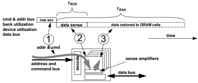
图一 Row access command and timing. tRAS 0: Row Access Strobe. The time interval between row access command and data restoration in a DRAM array. A DRAM bank cannot be precharged until at least tRAS time after the previous bank activation. 从Row Active Command的assertion开始的tRCD时间之后,数据在Sense Amplifier上可用,但尚未完全restored到DRAM cell。DRAM 从接收到 Row Active Command 到完成 Row restore 操作所需要的时间定义为 tRAS(the Row Access Strobe latency)。从Row Active Command的assertion开始的tRAS时间之后,假设感知放大器已完成对DRAM阵列的数据restore,然后可以对Sense Amplifier进行precharge,以便对DRAM阵列中同一bank的不同行进行访问。如图一所示。
tCAS 1: Column Access Strobe latency. The time interval between column access command and the start of data return by the DRAM device(s). Also known as tCL. Controller 在发送 Row Active Command后的tRCD时间之后,bank处于激活状态,Sense Amplifier中有完整的page内容,接着发送Column Read Commond进行数据读取。Column Read Command 通过数据总线指明需要读取的 Column 的起始地址。与列读取命令相关的三个基本计时参数是:tCAS、tCCD和tBURST。DRAM设备在发出列读取命令后将请求的数据放到数据总线上所需的时间,定义为tCAS(CAS for Column Address Strobe),也称为tCL。如图二所示。
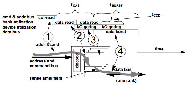
图二 Column-read command and timing. tBURST 4: Data burst duration. The time period that data burst occupies on the data bus. Typically 4 or 8 beats of data. In DDR SDRAM, 4 beats of data occupy 2 full clock cycles. tCAS时间之后,紧接着就是数据burst阶段,数据从预取缓冲区逐个发往IO总线,经过四个时钟周期发送完毕。这一时间定义为tBURST,表示数据burst周期。对同一bank的后续读取必须至少间隔tBURST,因为至少需要tBURST才能将预取缓冲区中的burst数据传输到IO总线。
tCCD 2: 一般为2或4,不超过tBURST。是列操作之间的最小时间间隔。Column-to-Column Delay. The minimum column command timing, determined by internal burst (prefetch) length. Multiple internal bursts are used to form longer burst for column reads. tCCD is 2 beats (1 cycle) for DDR SDRAM, and 4 beats (2 cycles) for DDR2 SDRAM. 现代DRAM设备在短时间内连续不断地传输数据。如图二,DRAM设备在内部以两个短的burst时间段移动数据,而在一个较长、连续的burst时间段将数据放在数据总线上。DRAM设备的内部burst长度在图二中标记为tCCD,单个列读取命令在数据总线上的数据burst持续时间标记为tBURST。定时参数tCCD表示最小burst持续时间的timing,或最小column-to-column命令timing。最小burst时间由DRAM设备的预取长度决定。例如,DDR SDRAM设备的预取长度为2 beats数据,因此tCCD在DDR SDRAM设备中是一个完整的时钟周期;DDR2 SDRAM设备的预取长度为4 beats数据,因此tCCD是DDR2 SDRAM设备的两个完整时钟周期。
tCWD 4: Column Write Delay. The time interval between issuance of the column-write command and placement of data on the data bus by the DRAM controller. Controller 在发送 Row Active Command后的tRCD时间之后,接着发送Write Commond进行数据写入。Column Write Command 通过地址总线指明需要写入数据的 Column 的起始地址。Controller 在发送完 Write Command 后,需要等待 tCWD (CWD for Column Write Delay) 时间后,才可以发送待写入的数据。所以从发送完Write Commond到发送待写入数据这段时间定义为tCWD, 在一些描述中也称为 tCWL(CWL for Column Write Latency)。
tWR 0: Write Recovery time. The minimum time interval between the end of a write data burst and the start of a precharge command. Allows sense amplifiers to restore data to cells. DRAM接收完数据后,需要一定的时间将数据写入到 DRAM Cells 中,这个时间定义为 tWR(WR for Write Recovery)。也称为write-to-precharge, PCM中不需要?
tRP 1: Row Precharge. The time interval that it takes for a DRAM array to be precharged for another row access. 在DRAM中,Refresh命令之前,每个bank必须要先Precharged,然后处于idle状态,从发出Precharge命令到激活同一bank中不同行之间所需的最小时钟周期数,称为一个tRP时延。
tRFC 100: Refresh Cycle time. The time interval between Refresh and Activation commands. Refresh时间,不在PCM中使用,但同样在配置文件中为其分配有效的数字。在一个Refresh命令完成后,所有的bank处于precharge (idle)状态,在Refresh命令和下一个activate命令(ACT)之间cycles数目必须大于等于tRFC(the Row Refresh Cycle Time )。
CLK 400: CPU运行频率为400MHz,那么周期为1/400 us=2.5ns。
tCWD 4: 10ns。Column Write Delay. The time interval between issuance of the column-write command and placement of data on the data bus by the DRAM controller. 不同的内存访问协议对tCWD有不同的设置。如图三所示,在SDRAM设备中,写数据与column-write命令同时放在数据总线上,tCWD为零。在DDR SDRAM设备中,tCWD被指定为内存系统中的一个时钟周期。在DDR2 SDRAM内存访问协议中,tCWD指定为比tCAS小一个周期,而在DDR3 SDRAM内存访问协议中,tCWD具有5到8个周期之间的可编程性。
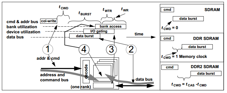
图三 Column-write command and timing for DDR SDRAM and DDR2 SDRAM devices.
原文作者: malizhen
原文链接: http://malizhen.github.io/2019/07/23/PCM-ISSCC-2012-4GB配置文件参数解析/
版权声明: 转载请注明出处(必须保留原文作者署名及原文链接)